¶ PINMUX
A number of GPIO pins between 2 and 31 have different possible applications. For example, GPIO8 can be connected to a signal wire for Serial GPIO, or it can be connected to a LAN port activity indicator, or it can be a manually controlled GPIO.
How it is configured depends significantly on how the specific board is wired. If in this example the board has Serial GPIO, then the physical pin will be wired to a 74HC595 or 74HC164 shift register chip, and the Serial GPIO configuration is the only one that makes sense.
However, if the board does not have Serial GPIO, then the physical pin is most likely wired to an LED, and the software may at times want to let that LED blink whenever there is activity on LAN port 2, and at other times the software may want to control that LED manually using the GPIO subsystem. The PINMUX allows for these configurations.
The GPIO pins and their possible functions are as follows:
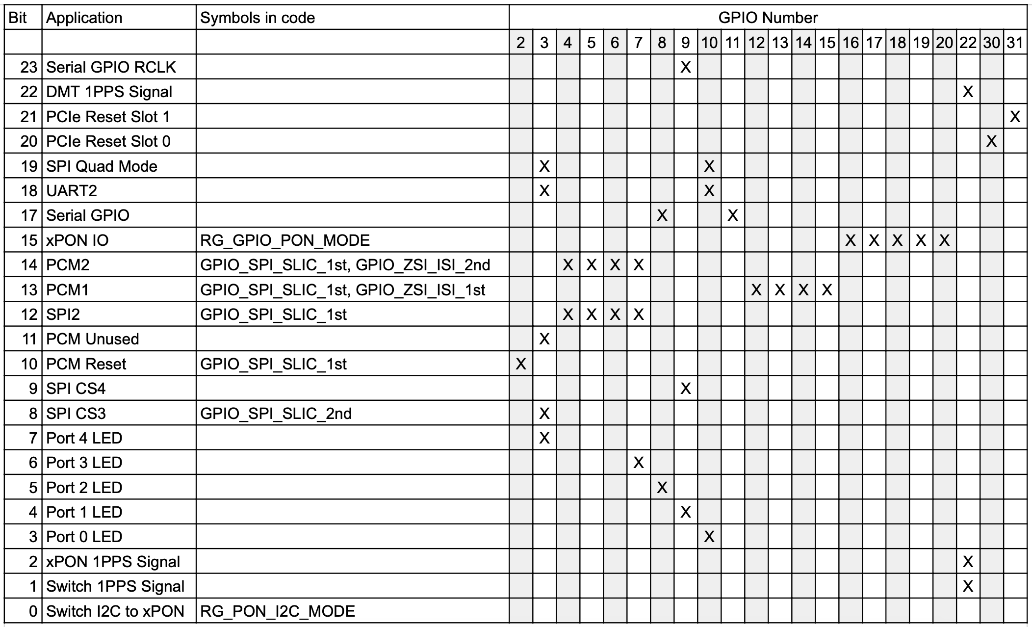
¶ Functions
¶ Serial GPIO
For boards which use a 74HC595 or 74HC164 shift register chip to expose an additional 17 GPIO outputs using only 2 (or 3) pins on the main chip.
- Uses: GPIO8, GPIO11
- Enable by setting bit 17
- Conflicts with: Port 2 LED
- If RCLK is required (74HC595) set bit 23
- Uses: GPIO9
- Conflicts with: SPI CS4
¶ 1PPS Signal
Output a timing reference from your choice three network subsystems.
- Uses: GPIO22
- Connect to xDSL DMT by setting bit 22
- Connect to xPON by setting bit 2
- Connect to Gigabit Switch by setting bit 1
¶ PCIe Reset Slot 1
If PCIe exists on the board, GPIO31 is wired as the slot 1 reset line.
- Uses: GPIO31
- Enable by setting bit 21
¶ PCIe Reset Slot 0
If PCIe exists on the board, GPIO30 is wired to the slot 0 reset line.
- Uses: GPIO30
- Enable by setting bit 20
¶ SPI Quad Mode
If the SPI Flash Controller is wired to the flash chip for quad mode, lines 3 and 10 are used in addition to the normal SPI lines.
- Uses: GPIO3, GPIO10
- Enable by setting bit 19
- Conflicts with: UART2, SPI CS3, PCM INT, Port4 LED, Port0 LED
¶ UART2
A second UART port is available, boards implementing this will use lines 3 and 10.
- Uses: GPIO3, GPIO10
- Enable by setting bit 18
- Conflicts with: SPI Quad Mode, SPI CS3, PCM INT, Port4 LED, Port0 LED
¶ xPON IO
Devices with EPON/GPON will use lines 16-20 to communicate with the PON subsystem.
- Uses: GPIO16, GPIO17, GPIO18, GPIO19, GPIO20
- Enable by setting bit 15
¶ PCM2
Devices with 2 VoIP phone jacks will use lines 4-7 to communicate with the 2nd VoIP subsystem.
- Uses: GPIO4, GPIO5, GPIO6, GPIO7
- Enable by setting bit 14
- Conflicts with: SPI2, Port3 LED
- NOTE: When communicating with a SLIC VoIP subsystem, the PCM driver enables both this and SPI2, so while they use the same GPIO pins, they are able to stay out of eachothers' way when used in coordination. Most likely, PCM data is only sent when SPI CS is disabled.
¶ PCM1
Devices with a VoIP phone jack will use lines 12-15 to communicate with the VoIP subsystem.
- Uses: GPIO12, GPIO13, GPIO14, GPIO15
- Enabled by setting bit 13
¶ PCM SPI2
The PCM subsystem contains an SPI interface that is used for communicating with SLIC chips such as Le9641 when in PCM-SPI mode. In principle, it can also be connected to any other type of SPI device. When enabled, it uses GPIOs 4-7. In ZSI mode, this is not necessary because control traffic is interleaved with PCM data.
- Uses: GPIO4, GPIO5, GPIO6, GPIO7
- Enable by setting bit 12
- Conflicts with: PCM2, Port3 LED
- Note: When communicating with a SLIC-SPI VoIP subsystem, the PCM driver enables both this and PCM2
¶ PCM INT
Line 3 can be connected to the SLIC subsystem to receive an interrupt when the SLIC has something to communicate, it avoids the need for polling.
- Uses: GPIO3
- Enabled by setting bit 11
- Conflicts with: SPI Quad Mode, UART2, SPI CS3, Port4 LED
¶ PCM Reset
For devices with a VoIP phone jack, pin 2 can be wired to the reset pin on the SLIC chip.
- Uses: GPIO2
- Enabled by setting bit 10
¶ PCM SPI CS4
This is probably the 3rd chip select line for the PCM SPI subsystem, with CS1 referring to the chip select line for the SPI Flash Controller.
- Uses: GPIO9
- Enabled by setting bit 9
- Conflicts with: Serial GPIO (RCLK), Port1 LED
¶ PCM SPI CS3
For boards has 2 VoIP phone jacks using SLIC-SPI mode, this chip select line allows enabling the 3nd SLIC chip for SPI communication.
- Uses: GPIO3
- Enabled by setting bit 8
- Conflicts with: SPI Quad Mode, UART2, PCM Interrupt, Port4 LED
¶ Port4 LED
If line 3 is wired to an LED light, it can be connected to the activity meter for LAN Port 4. This is one pin which makes sense to configure at runtime, for example when switching an LED between showing network activity, and manually controlling it to display a pattern e.g. during startup or software update.
- Uses: GPIO3
- Enabled by setting bit 7
- Conflicts with: SPI Quad Mode, UART2, PCM Interrupt, PCM SPI CS3
- Note: While these ports are called Port0-Port4, their mapping to the actual LAN ports can be changed by another configuration register.
¶ Port3 LED
Activity indicator for LAN port 3
- Uses: GPIO7
- Enabled by setting bit 6
- Conflicts with: SPI2, PCM2
- See: Port4 LED for additional details
¶ Port2 LED
Activity indicator for LAN port 2
- Uses: GPIO8
- Enabled by setting bit 5
- Conflicts with: Serial GPIO
- See: Port4 LED for additional details
¶ Port1 LED
Activity indicator for LAN port 1
- Uses: GPIO9
- Enabled by setting bit 4
- Conflicts with: Serial GPIO (RCLK), PCM SPI CS4
- See: Port4 LED for additional details
¶ Port0 LED
Activity indicator for LAN port 0
- Uses: GPIO10
- Enabled by setting bit 3
- Conflicts with: UART2, SPI Quad Mode
- See: Port4 LED for additional details
¶ Route I2C to xPON
This doesn't occupy any known GPIO pins, it seems to change the output of the I2C subsystem, making it communicate with the xPON subsystem rather than the standard I2C output pins.
- Enabled by setting bit 0